Re-published from The Journal of Physical Chemistry Letters
Jingya Sun, Aniruddha Adhikari, Basamat S. Shaheen, Haoze Yang, and Omar F. Mohammed*
Solar and Photovoltaics Engineering Research Center, Division of Physical Sciences and Engineering, King Abdullah University of Science and Technology, Thuwal 23955-6900, Kingdom of Saudi Arabia
 ABSTRACT:
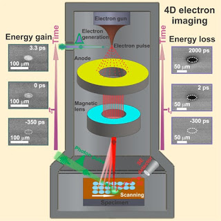
Selectively capturing the ultrafast dynamics of charge carriers on materials surfaces and at interfaces is crucial to the design of solar cells and optoelectronic devices. Despite extensive research efforts over the past few decades, information and understanding about surface-dynamical processes, including carrier trapping and recombination remains extremely limited. A key challenge is to selectively map such dynamic processes, a capability that is hitherto impractical by time-resolved laser techniques, which are limited by the laser’s relatively large penetration depth and consequently these techniques record mainly bulk information. Such surface dynamics can only be mapped in real space and time by applying four-dimensional (4D) scanning ultrafast electron microscopy (S-UEM), which records snapshots of materials surfaces with nanometer spatial and subpicosecond temporal resolutions. In this method, the secondary electron (SE) signal emitted from the sample’s surface is extremely sensitive to the surface dynamics and is detected in real time. In several unique applications, we spatially and temporally visualize the SE energy gain and loss, the charge carrier dynamics on the surface of InGaN nanowires and CdSe single crystal and its powder film. We also discuss the mechanisms for the observed dynamics, which will be the foundation for future potential applications of S-UEM to a wide range of studies on material surfaces and device interfaces.